Request a solution
KLA Instruments - Logo
KLA Instruments

Areas of application:

Filmetrics® F54-XY-200 and F54-XY-300

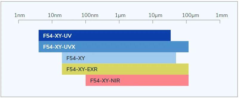
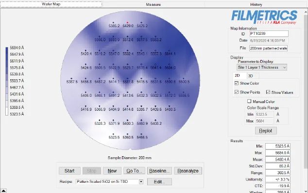
The Filmetrics® F54-XY series provides automated mapping of thin film thickness, refractive index, reflectivity, absorption, and surface roughness on samples up to 300 mm. It offers five configurations with measurement ranges from 4 nm to 120 µm and spot sizes from 2 µm to 100 µm.

Key Features

  • Support for both structured and unstructured samples
  • Configurations with wavelength ranges from 190 to 1700 nm
  • Minimum measuring spot size of 5 µm
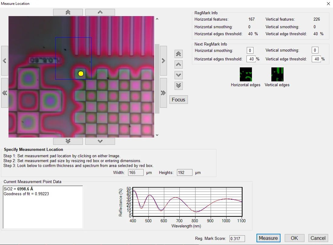
  • Autofocus and pattern recognition
  • Safety cover with interlock
  • Live video image
  • Support for samples up to 300 mm in diameter
  • User-definable mapping points (rectangular, linear, polar, and custom configurations)
  • Manual or automatic sample alignment
  • Advanced history for saving, reproducing, and plotting results
  • Built-in reference and thickness standards
  • Extensive material library and advanced modeling algorithms
Richard Schuster
Expert advisor

Ing. Richard Schuster

+420 601 123 593

schuster@optixs.cz

Send inquiry

OptiXs care

  • We will expertly consult your planned application
  • Our team is able to integrate the product into a larger system
  • We ensure fast delivery of spare parts and local service
What else we can help with

Product description

The Filmetrics® F54-XY-200 and F54-XY-300 automated systems measure the thickness of thin layers on structured and unstructured samples up to 200 mm and 300 mm in diameter, respectively. Mapping is performed using an advanced spectral reflectance system and Filmetrics algorithms.

The compact system brings accurate measurement positioning to manufacturing applications. The motorized XY-200 stage automatically moves to specified measurement locations and provides results at a rate of up to two points per second. Measurement of 300 mm diameter wafers is supported by an additional high-performance rotary stage in the F54-XYT-300 configuration.

Applications

  • Semiconductor process films – measurement of the thickness of polysilicon, photoresists, oxides, nitrides, and SOI layers; measurement of thinned silicon.
  • Compound semiconductors – measurement of thickness and optical properties of layers and wafers (e.g., GaN, SiC).
  • LCD displays – measurement of cell gaps and thickness of polyimides, ITO and TCO layers.
  • Optical coatings and electro-optical films – measurement of the thickness of hardcoats, anti-reflective layers, and filters (modeling of more than 10 layers).
  • Coatings for medical applications – measurement of the thickness and homogeneity of parylene and other protective coatings on implants; possibility of automated measurement of sample fields.
  • MEMS – measuring the thickness of photoresists, silicon membranes, and dielectric layers, mapping homogeneity to detect defects.

Parameters

F54-XY configuration – select the appropriate model according to the measurement range
Model Thickness range* Spectral range
F54-XY 20 nm – 50 µm 380 – 1050 nm
F54-XY-UV 4 nm – 35 µm 190 – 1100 nm
F54-XY-NIR 100 nm – 120 µm 950 – 1700 nm
F54-XY-EXR 20 nm – 120 µm 380 – 1700 nm
F54-XY-UVX 4 nm – 120 µm 190 – 1700 nm

* Depending on the material and lens.

Accessories

Standards for film thickness
Film thickness standards – NIST-traceable standards for calibration and accuracy verification

Inquire product

Are you interested in product? Send us your requirements via the enquiry form or contact an expert consultant directly. We will be happy to answer your questions and propose a solution according to your needs.

Expert advisor

Richard Schuster

Ing. Richard Schuster