
Request a solution
KLA Instruments - Logo
KLA Instruments

Areas of application:

Filmetrics® F54

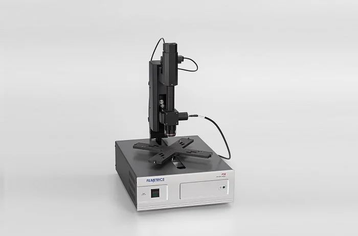
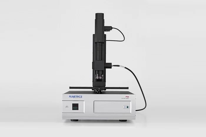
Filmetrics® F54 combines the microscopic measurement spot size of the F40 instrument with an integrated camera and automated sample mapping up to 450 mm diameter using an R-Theta stage and advanced spectral reflectance system.

Key Features

  • Microscopic measurement spot size
  • Integrated live view camera
  • Autofocus (motorized Z-axis)
  • Intuitive FILMeasure software included with every system
  • Complete package including spectrometer with light source, microscope adapter, reference and calibration standards
Richard Schuster
Expert advisor

Ing. Richard Schuster

+420 601 123 593

schuster@optixs.cz

Send inquiry

OptiXs care

  • We will expertly consult your planned application
  • Our team is able to integrate the product into a larger system
  • We ensure fast delivery of spare parts and local service
What else we can help with

Product description

Filmetrics® F54 enables quick and easy mapping of thin film thicknesses on samples up to 450 mm. The motorized R-Theta stage automatically moves to selected measurement points and provides measurements at speeds of up to two points per second. Autofocus and microscopic measurement point size are standard features of this advanced system.

The instrument can be connected to a user's laptop in minutes and ready to measure. The system includes dozens of predefined mapping patterns (polar, rectangular, or linear), with the ability to create custom patterns with an unlimited number of measurement points.

Applications

  • Semiconductors – amorphous and polysilicon: measurement of optical constants (n and k) and thickness of layers and sublayers, including SiO₂, with a single click.
  • Semiconductors – Dielectrics: Measure the thickness of SiO₂ (from 3 nm to 1 mm), the refractive index of Si₃N₄, and other dielectric layers.
  • Displays – ITO/TCO layers: measurement of indium tin oxide layers, polyimides, hardcoats, LCD and OLED layers.
  • Coatings for medical applications: catheters, balloons, stents, conductors, needles, implants, including coatings for drug delivery.
  • OLED displays: robust, non-contact metrology of prototypes and fully pixelated displays, possibility of detecting chemical changes.
  • Photoresists: thickness and etching rate of single-layer and multi-layer structures (e.g., SU-8, Dow BCB).
  • Porous silicon: unique algorithm for measuring layer thickness, index, and porosity.
  • Silicon wafers and membranes: measurement of the thickness of wafers and membranes made of materials such as Si, sapphire, quartz glass, SiC, LiTaO₃, GaN, glass.

Parameters

Select the right Filmetrics F54 configuration for your measurements

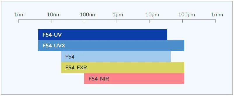
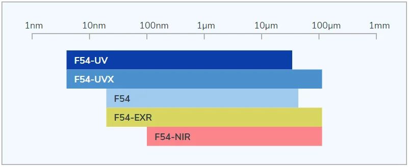
The F54 configuration differs primarily in the thickness measurement range, which is determined by the spectral range of the instrument. Shorter wavelengths (F54-UV) are necessary for measuring thinner layers, while longer wavelengths are required for measuring coarser, thicker, and more opaque layers.

Filmetrics® F54

Model Thickness range* Spectral range
F54 20 nm – 45 µm 380 – 1050 nm
F54-UV 4 nm – 35 µm 190 – 1100 nm
F54-NIR 100 nm – 115 µm 950 – 1700 nm
F54-EXR 20 nm – 115 µm 380 – 1700 nm
F54-UVX 4 nm – 115 µm 190 – 1700 nm

* Depending on the material and lens.

Accessories

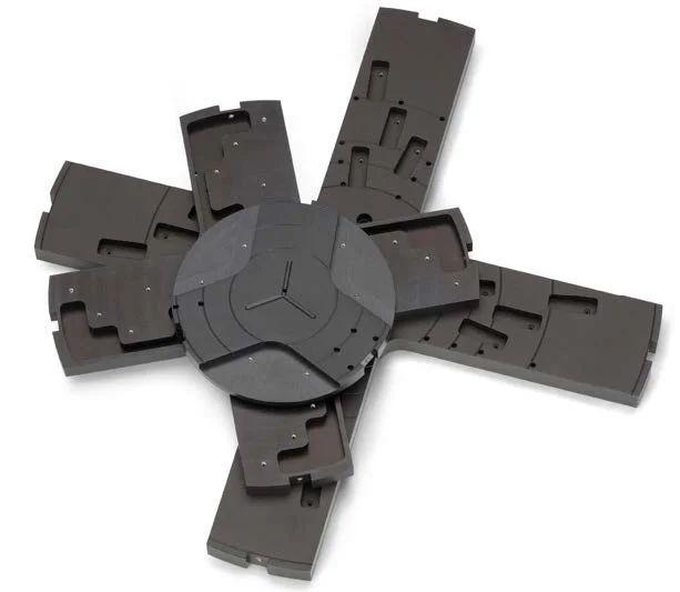
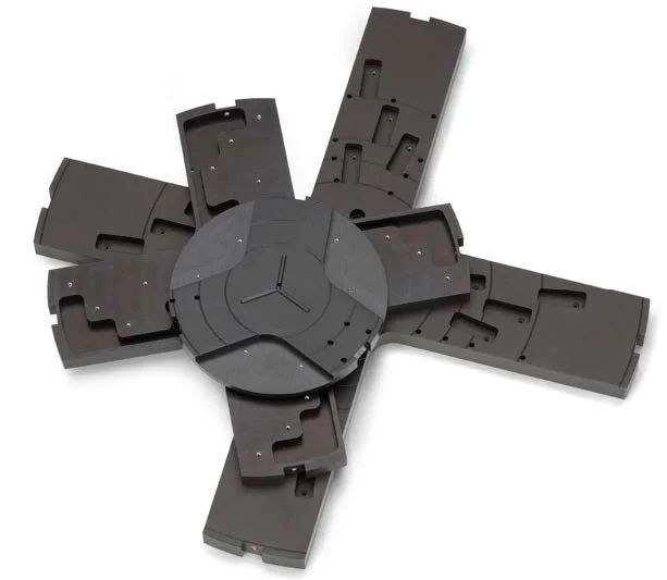
F50 Chuck
F50 Chuck – wafer clamping holders
(2”, 3”, 4”, 5”, 6”, 200 mm, 300 mm, 450 mm)
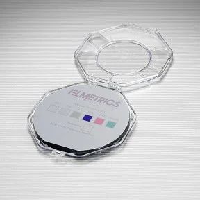
Standardy pro tloušťku filmů
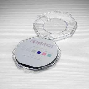
Film thickness standards
NIST-traceable standards for calibration and accuracy verification

Inquire product

Are you interested in product? Send us your requirements via the enquiry form or contact an expert consultant directly. We will be happy to answer your questions and propose a solution according to your needs.

Expert advisor

Richard Schuster

Ing. Richard Schuster