We distribute this product only in the Czech Republic and Slovakia.

Nano Indenter® G200X

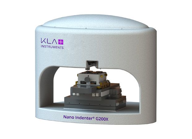
The Nano Indenter® G200X is an easy-to-use nanoscale mechanical property tester that quickly provides accurate and quantitative results. It allows testing of a wide range of samples, from hard coatings to soft polymers, and offers the most comprehensive set of tests in KLA Instruments' nanoindenter product line.

Key Features

  • Electromagnetic actuator with high dynamic range of force and displacement
  • High-resolution optical microscope and precise XYZ motion system
  • Easy-to-use multi-position sample stage for high measurement throughput
  • Modular testing options: SPM imaging, scratch tests, high-temperature measurements, dynamic tests (CSM), high-speed tests
  • Intuitive user interface and quick test setup
  • Real-time experiment control, easy protocol development and test configuration
  • InView software including ReviewData and InFocus for data analysis and report generation
  • Award-winning high-speed testing for material property mapping
  • InQuest electronics with 100 kHz data acquisition speed and 20 µs time constant
Richard Schuster
Expert advisor

Ing. Richard Schuster

+420 601 123 593

schuster@optixs.cz

Send inquiry

OptiXs care

  • We will expertly consult your planned application
  • Our team is able to integrate the product into a larger system
  • We ensure fast delivery of spare parts and local service
What else we can help with

Product description

The Nano Indenter® G200X is a versatile system for mechanical testing at the nanoscale. It includes a high-performance motion system, a large sample mounting system, and a high-resolution optical microscope. The InView software platform, InQuest controller, and InForce actuators ensure consistently high-quality results across the product line.

Optional features include continuous stiffness measurement (CSM), scanning probe microscopy, scratch tests, frequency characterization, electrical measurements, high-speed testing, and impact testing. The new G200X Semi Pack offers advanced solutions for characterizing layers in the semiconductor and compound industries.

Applications

  • Fast measurement of hardness and modulus of elasticity (Oliver-Pharr)
  • High-speed mapping of material properties
  • Determination of yield stress/strain
  • Hardness tests according to ISO 14577
  • Measurement of thin layers and coatings
  • Measurement of layer adhesion and delamination
  • Measurement of fracture toughness (stiffness mapping, CSM, NanoVision)
  • Viscoelastic properties (tan δ, storage and loss modulus)
  • Scanning probe microscopy (3D imaging)
  • Quantitative scratch and wear tests
  • Nanoindentation at elevated temperatures
  • Electrical measurements (I-V characteristics)

Industry

  • Semiconductor industry
  • Universities, research laboratories, and institutes
  • PVD/CVD hard coatings (e.g., DLC, TiN)
  • MEMS – microelectromechanical systems, universal testing at the nanoscale
  • Ceramics and glass
  • Metals and alloys
  • Biomaterials and pharmaceutical materials
  • Coatings and paints
  • Composites
  • Batteries and energy storage systems
  • Automotive and aerospace industries

Inquire product

Are you interested in product? Send us your requirements via the enquiry form or contact an expert consultant directly. We will be happy to answer your questions and propose a solution according to your needs.

Expert advisor

Richard Schuster

Ing. Richard Schuster