Request a solution
KLA Instruments - Logo
KLA Instruments

Areas of application:

Measurement of step height, roughness, curvature, and stress in thin layers

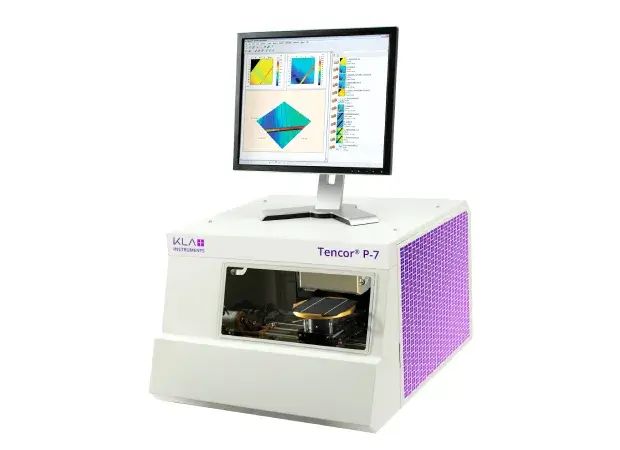
Tencor® P-7 Stylus Profiler

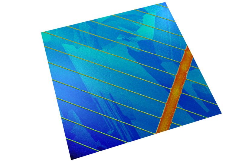
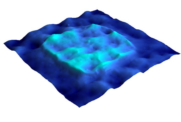
The Tencor® P-7 is a benchtop stylus profilometer with a step height measurement range from a few nanometers up to 1 mm. It supports 2D and 3D measurement of height, roughness, curvature, and stress without the need for image stitching for scans up to 150 mm.

Key Features

  • Step height range: from nanometers to 1000 µm
  • Constant force control: 0.03 to 50 mg
  • Measurement of the entire sample area without stitching (up to 150 mm)
  • 5MP high-resolution color camera
  • Arc correction – elimination of errors caused by arc movement of the tip
  • User-friendly software interface
  • Fully automated operation with sequencing, pattern recognition, and SECS/GEM support

Richard Schuster
Expert advisor

Ing. Richard Schuster

+420 601 123 593

schuster@optixs.cz

Send inquiry

OptiXs care

  • We will expertly consult your planned application
  • Our team is able to integrate the product into a larger system
  • We ensure fast delivery of spare parts and local service
What else we can help with

Product description

The Tencor® P-7 is based on the successful Tencor P-17 system and offers its accuracy in a compact benchtop platform with an excellent price/performance ratio. The instrument enables 2D and 3D measurements of step height, roughness, curvature, and stress of thin films in scans up to 150 mm without stitching.

Thanks to constant force technology, the P-7 is capable of accurately measuring even soft materials such as photoresists. The system is suitable for both research and manufacturing applications.

Applications

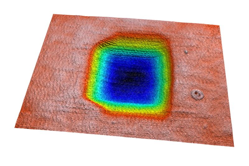
  • Step Height: 2D and 3D measurement of step height from nanometers to 1000 µm – for etching, sputtering, deposition, spin coating, or CMP processes.
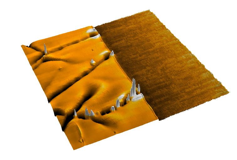
  • Texture: roughness and waviness measurement (2D and 3D), software filters separate individual components and calculate parameters such as RMS roughness.
  • Form: measurement of surface curvature and shape (2D and 3D), including measurement of wafer or optical lens curvature.
  • Stress: measurement of thin film stress (2D and 3D) using surface curvature changes; calculation according to Stoney's equation.
  • Defect Review: measurement of defect topography (e.g., scratches) based on KLARF files from inspection systems.

Industry

  • Universities, research laboratories, and institutes
  • Semiconductor and compound semiconductor industry
  • LEDs (light-emitting diodes)
  • Solar technology
  • MEMS – microelectromechanical systems
  • Data storage
  • Automotive industry
  • Medical devices

Inquire product

Are you interested in product? Send us your requirements via the enquiry form or contact an expert consultant directly. We will be happy to answer your questions and propose a solution according to your needs.

Expert advisor

Richard Schuster

Ing. Richard Schuster