
We are a technically and knowledgeable partner for scientific and industrial applications

Společnost Quantum Design International, Inc., přední dodavatel vědecké instrumentace, oznámila akvi...
Andor has introduced a new series of CB2 sCMOS cameras that expand the possibilities of scientific i...
Working with lasers requires 100% eye protection. Laser radiation is invisible and can cause permane...
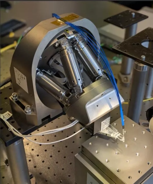
The new Piezo Gripper P-606.1P from PI offers nanometer-level precision, fast response, and stable h...
As part of Laser Safety Week, we invite you to a free online webinar, "Laser Safety in Practice," wh...
May 16th marks exactly 66 years since the first functional laser in the world was launched. This sig...
For us, collaboration means more than just delivering a system. We care about your project
and strive to provide the best possible solution for your needs. That's why we automatically and without
compromise provide comprehensive care in every collaboration, whether it's expert consultation, sample
testing, training or a superior warranty.
News
Show all
Science and research
Quantum Design completes its second acquisition of 2026 – it is taking over Qnami
 Science and research
New from Andor: CB2 sCMOS cameras for cutting-edge scientific imaging
 Science and research
Certified glasses: Reliable eye protection
 Show all
Industry and manufacturing
PI has introduced the Piezo Gripper P-606.1P: a new standard for highly dynamic photonic applications
 Industry and manufacturing
Free WEBINAR: Laser Safety in Practice
 Industry and manufacturing
Laser safety week in OptiXs

OptiXs care
Creation of a local clean environment for working with a packaging machine in a 1.5 x 1.5 m enclosure equipped with a single flow module. The customer's requirement was to ensure the safety of the room and the optical bench and to design the system for use with Class 4 lasers. The system was to allow operation in various safety modes. A cleanroom for dusty environments with ISO 5 air filtration, custom design, installation, and commissioning for demanding high-tech manufacturing. The client requested a confocal Raman microscope with computer-controlled adjustment of the physical confocal aperture in the range of at least 25 µm to 100 µm. The customer needed an active anti-vibration floor for a planned electron microscope, which would be an integral part of the newly built, renovated workplace or laboratory floor. Scientists in the MEL (Materials-Envi Lab) group led by Professor Zbořil at the Center for Nanotechnology at VŠB-TUO are actively engaged in electron paramagnetic resonance (EPR) spectroscopy and its applications in modern low-dimensional materials. In semiconductor manufacturing, rapid and reliable wafer quality screening is critical to protecting yield and accelerating production. Traditional inspection methods, such as optical microscopy or electrical testing, provide limited insight into subsurface structures and material heterogeneities, which can lead to device performance variability or downstream failures. The assembly of certain industrial equipment, such as components or precision mechanics, requires a dust-free environment. However, these parts often have to be assembled in ordinary production halls or workshops where dust is naturally generated by the surrounding operations. The production and handling of optoelectronic components, crystals and precision optics require a contamination-free environment. Even a microscopic dust particle can damage a surface or cause a defect in an optical system.
Our experience grows with every project.
We carry out more than 800 projects a year.


 All references

Custom manufacturing of cleanroom enclosures

Laboratory Safety and Table Covers

Clean cell for dusty environments

Confocal Raman microscope with FLIM module

Active anti-vibration system STACIS 4

Beam combiner for EPR spectrometer
Application
Show All
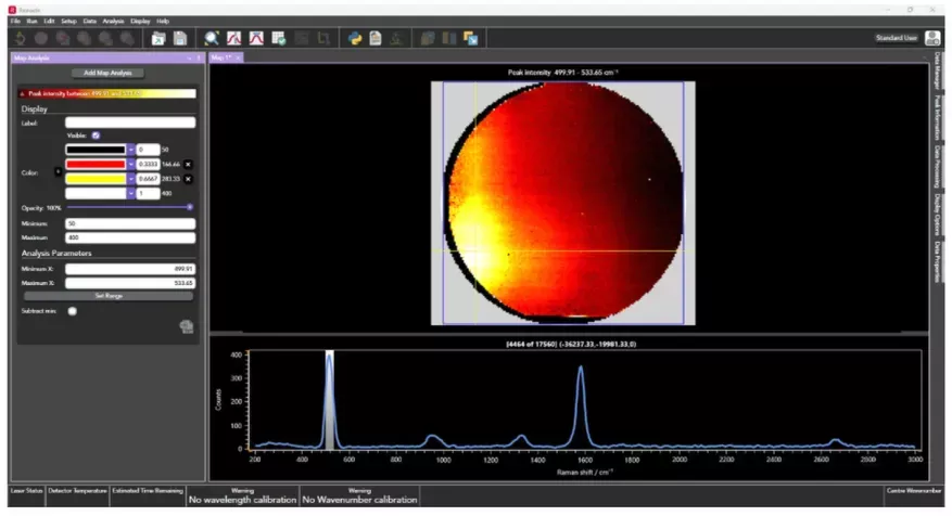
Raman-Based Semiconductor Wafer Quality Assurance Using the RMS1000 and WaferMAP
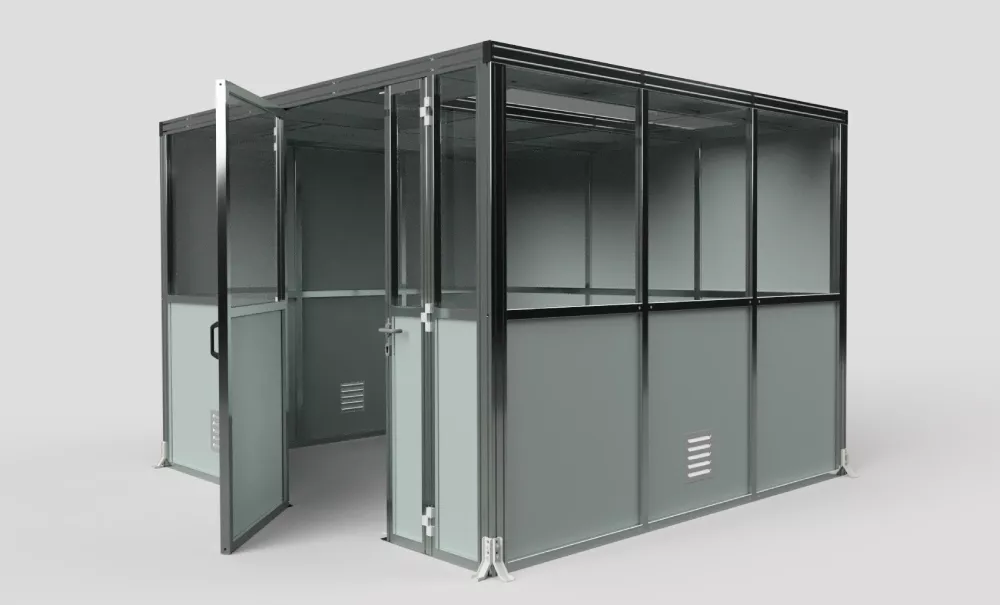
Clean zone in a standard production hall: Assembly of sensitive parts in a dusty environment
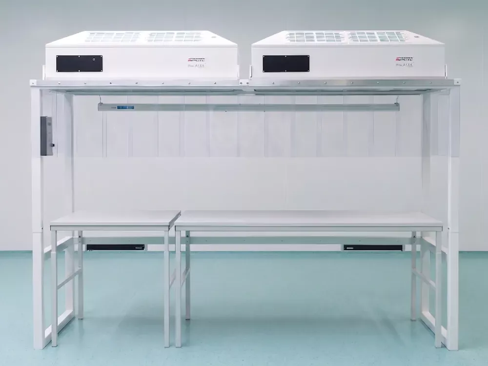
Local clean environment for packaging and assembly in optics and optoelectronics
Need help with your application? Contact us to find out how our expertise can strengthen your project.